Product Description
Features
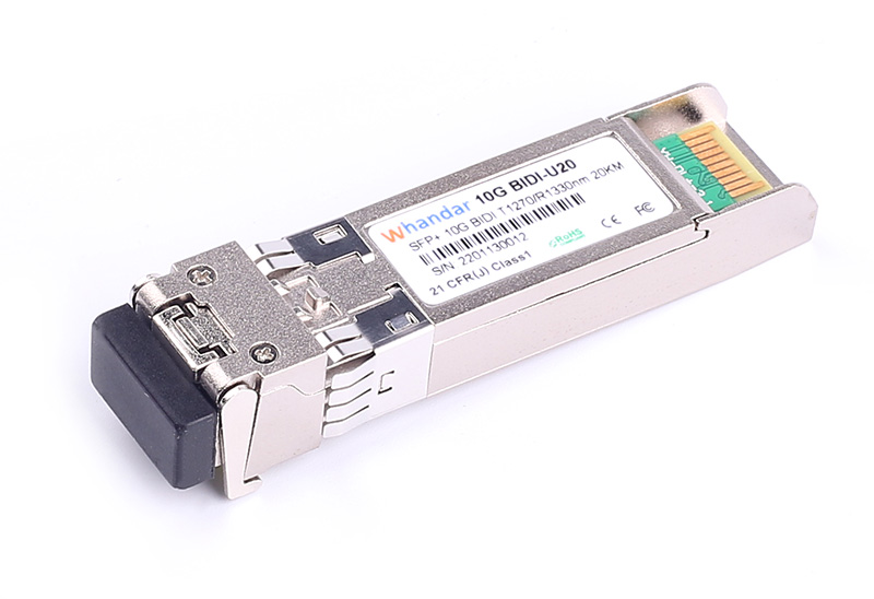
Hot-pluggable SFP footprint
Simplex LC fiber connector
Transmission distance up to 20Km on 9/125µm SMF
Built-in DDMI functions
Comply with SFP MSA .
Single +3.3V power supply
RoHS6 compliant (lead free)
Operating case temperature:
Commercial : 0 to +70°C
Industrial : -40 to +85°C
Comply with Ethernet Switches from a lot of widely used brands .
Applications
10GBASE Ethernet
SONET OC-192 SDH STM-64
Switch to Switch interface
Router/Server interface
Other optical transmission systems
Optical Parameters
HD-SFP+/10G-BIDI-20U:(1270nm TX/1330nm RX)
Parameter | Symbol | Min. | Typical | Max. | Unit | Note |
Transmitter Section: |
Center Wavelength | λt | 1260 | 1270 | 1280 | nm |
|
Side Mode Suppression Ratio | SMSR | 30 | - | - | dB |
|
Average Optical Power | Pavg | -3.0 |
| +3 | dBm |
|
Laser Off Power | Poff | - | - | -30 | dBm |
|
Extinction Ratio | ER | 3.5 | - | - | dB |
|
Transmitter Dispersion Penalty | TDP | - | - | 3.2 | dB |
|
Relative Intensity Noise | Rin | - | - | -128 | dB/Hz | 12dB reflection |
Optical Return Loss Tolerance |
| - | - | 12 | dB |
|
Receiver Section: |
|
Center Wavelength | λr | 1320 |
| 1340 | nm |
|
Receiver Sensitivity in Average Power | Sen |
|
| -14.4 | dBm | 1 |
Vertical eye closure penalty |
| 2.2 | - | - | dB | 3 |
Los Assert | LosA | -30 | - | - | dBm |
|
Los Dessert | LosD | - | - | -16.0 | dBm |
|
Los Hysteresis | LosH | 0.5 | - | - | dB |
|
Overload | Pin | - | - | 0.5 | dBm | 1 |
Receiver Reflectance |
| - | - | -12 | dB |
|
Stressed eye jitter |
| 0.3 | - | - | UIp-p | 2 |
Receive electrical 3dB upper cutoff frequency |
| - | - | 12.3 | GHz |
|
Receiver power (damage) |
| - | - | 1.5 | dBm |
|
Optical Parameters
HD-SFP+/10G-BIDI-20D:(1330 TX/1270 nm RX )
Parameter | Symbol | Min. | Typical | Max. | Unit | Note |
Transmitter Section: |
Center Wavelength | λt | 1320 | 1330 | 1340 | nm |
|
Side Mode Suppression Ratio | SMSR | 30 | - | - | dB |
|
Average Optical Power | Pavg | -3.0 |
| +3 | dBm |
|
Laser Off Power | Poff | - | - | -30 | dBm |
|
Extinction Ratio | ER | 3.5 | - | - | dB |
|
Transmitter Dispersion Penalty | TDP | - | - | 3.2 | dB |
|
Relative Intensity Noise | Rin | - | - | -128 | dB/Hz | 12dB reflection |
Optical Return Loss Tolerance |
| - | - | 12 | dB |
|
Receiver Section: |
|
Center Wavelength | λr | 1260 |
| 1280 | nm |
|
Receiver Sensitivity in Average Power | Sen |
|
| -15.0 | dBm | 1 |
Vertical eye closure penalty |
| 2.2 | - | - | dB | 3 |
Los Assert | LosA | -30 | - | - | dBm |
|
Los Dessert | LosD | - | - | -12 | dBm |
|
Los Hysteresis | LosH | 0.5 | - | - | dB |
|
Overload | Pin | - | - | 0.5 | dBm | 1 |
Receiver Reflectance |
| - | - | -12 | dB |
|
Stressed eye jitter |
| 0.3 | - | - | UIp-p | 2 |
Receive electrical 3dB upper cutoff frequency |
| - | - | 12.3 | GHz |
|
Receiver power (damage) |
| - | - | 1.5 | dBm |
|
Notes:
1. Average optical power shall be measured using the methods specified in TIA/EIA-455-95.
2. Receiver sensitivity is informative. Stressed receiver sensitivity shall be measured with conformance test signal for BER =1x 10-12 .
3. Vertical eye closure penalty and stressed eye jitter are the test conditions for measuring stressed receiver sensitivity. They are not the required characteristic of the receiver.
4. Power budget is defined as the different between the Rx sensitivity and the Tx output power of the interface.
5. Path penalty is intended as the power penalty of the interface between back-to-back and the maximum applied dispersion.
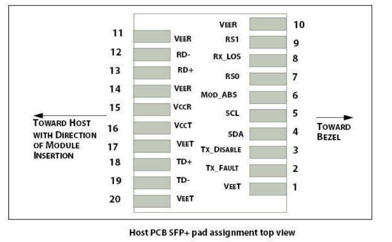
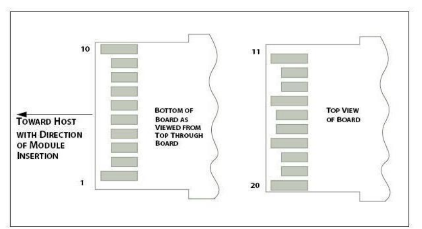
Pin Assignment:
Pin Descriptions
PIN | Logic | Symbol | Name / Description | Note |
1 |
| VeeT | Module Transmitter Ground | 1 |
2 | LVTTL-O | TX_Fault | Module Transmitter Fault |
|
3 | LVTTL-I | TX_Dis | Transmitter Disable; Turns off transmitter laser output |
|
4 | LVTTL-I/O | SDA | 2-Wire Serial Interface Data Line | 2 |
5 | LVTTL-I | SCL | 2-Wire Serial Interface Clock | 2 |
6 |
| MOD_DEF0 | Module Definition, Grounded in the module |
|
7 | LVTTL-I | RS0 | Receiver Rate Select |
|
8 | LVTTL-O | RX_LOS | Receiver Loss of Signal Indication Active LOW |
|
9 | LVTTL-I | RS1 | Transmitter Rate Select (not used) |
|
10 |
| VeeR | Module Receiver Ground | 1 |
11 |
| VeeR | Module Receiver Ground | 1 |
12 | CML-O | RD- | Receiver Inverted Data Output |
|
13 | CML-O | RD+ | Receiver Data Output (not used) |
|
14 |
| VeeR | Module Receiver Ground | 1 |
15 |
| VccR | Module Receiver 3.3 V Supply |
|
16 |
| VccT | Module Receiver 3.3 V Supply |
|
17 |
| VeeT | Module Transmitter Ground | 1 |
18 | CML-I | TD+ | Transmitter Non-Inverted Data Input |
|
19 | CML-I | TD- | Transmitter Inverted Data Input |
|
20 |
| VeeT | Module Transmitter Ground | 1 |
SFP+ Module PIN Definition
Notes:
1. Module ground pins GND are isolated from the module case.
2. Shall be pulled up with 4.7K-10Kohms to a voltage between 3.15V and 3.45V on the host board.
Ordering information
Part Number | Product Description |
HD-SFP+/10G-BIDI-20U | 1270nm TX/1330nm RX, 10Gbps, 20Km, 10Gbps SFP+ Bi-Directional Transceiver with Single LC Receptacle, 0ºC ~ +70ºC . |
HD-SFP+/10G-BIDI-20D | 1330nm TX/1270nm RX, 10Gbps, 20Km, 10Gbps SFP+ Bi-Directional Transceiver with Single LC Receptacle, 0ºC ~ +70ºC . |
HD-SFP+/10G-BIDI-20UI | 1270nm TX/1330nm RX, 10Gbps, 20Km, 10Gbps SFP+ Bi-Directional Transceiver with Single LC Receptacle, -40ºC ~ +85ºC . |
HD-SFP+/10G-BIDI-20DI | 1330nm TX/1270nm RX, 10Gbps, 20Km, 10Gbps SFP+ Bi-Directional Transceiver with Single LC Receptacle, -40ºC ~ +85ºC . |





 sales@huahanda.com
 0755-86654236