click to view bigger image
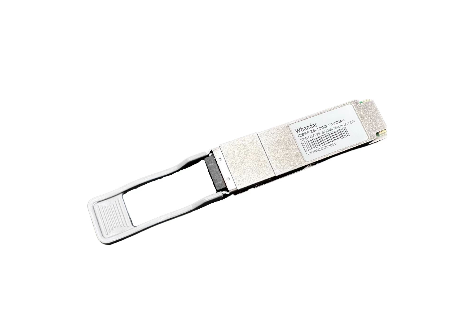
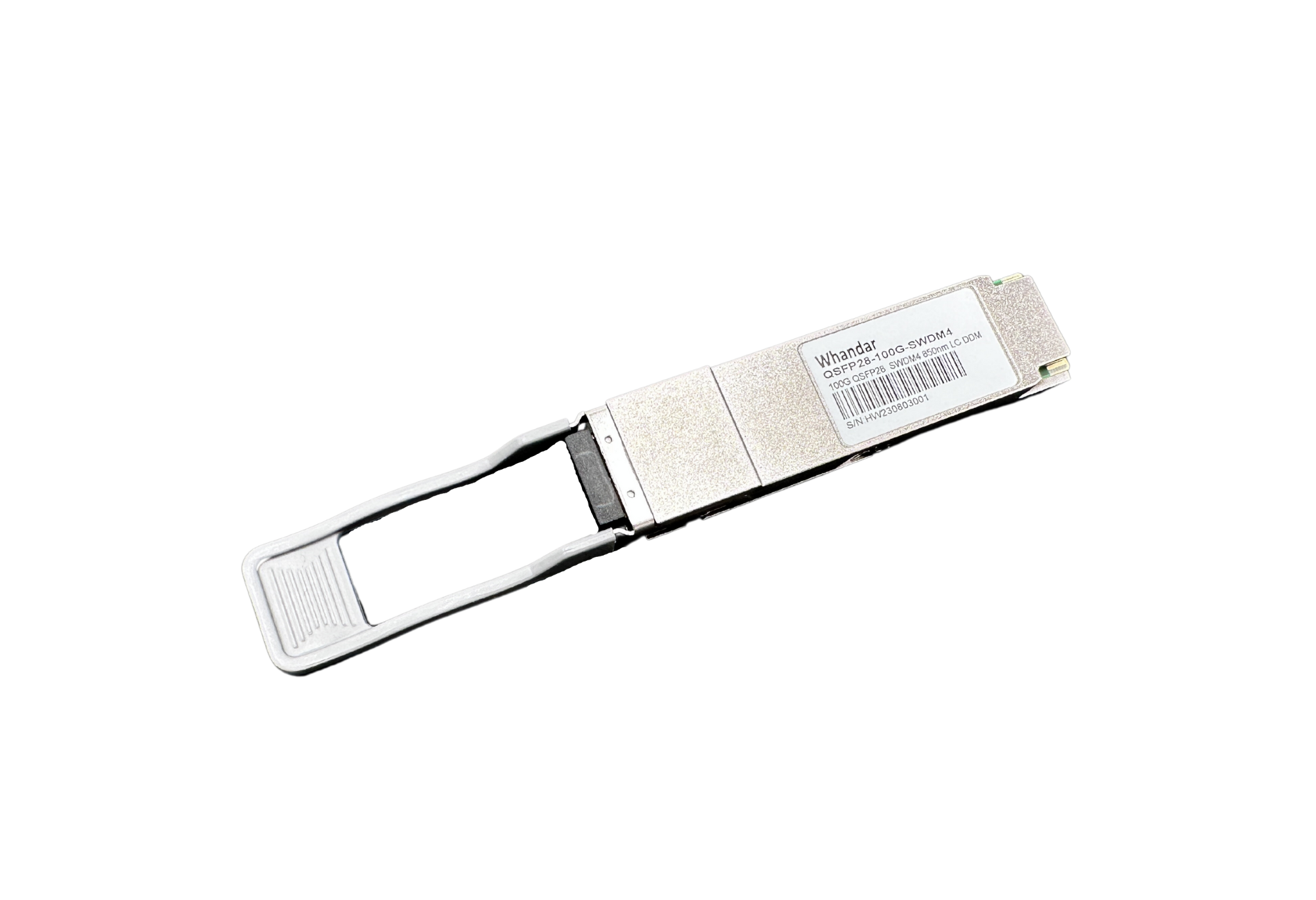
100G QSFP28 SWDM4 Optical Transceiver
Support hotline:
0755-86654236 /
Product Details
Product Description
The 100G QSFP28 SWDM4 transceiver modules are designed for use in 100G Ethernet links over duplex multimode fiber. Four channels/lanes in the 850-940nm region @ 25.78Gbps to transport the Ethernet signal. Digital diagnostics functions are available via an I2C interface, as specified by the QSFP28 MSA.
Applications
ü 100G Ethernet over Duplex MM
Feature
ü Compliant with QSFP28 MSA
ü Compliant with SWDM MSA
ü Compliant with IEEE802.3bm CAUI-4
ü Hot-pluggable QSFP28 form factor
ü 4x25Gb/s 850mm VCSEL-based transmitter
ü Supports 103.1Gbps aggregate bit rate
ü Power dissipation<3.5W
ü Maximum link length of 150m on OM5 multimode Fiber
ü Case temperature range of 0°C to 70°C
ü Duplex LC receptacles
ü CAUI-4 electrical interface
ü RoHS compliant
Absolute Maximum Ratings
Parameter | Symbol | Min | Max | Units |
Storage Temp Range | Ts | -40 | +85 | ℃ |
Supply Voltage | Vcc | -0.5 | 3.6 | V |
Relative Humidity | RH | 15% | 85% |
Operating Conditions
Parameter | Symbol | Min | Max | Units |
Case Temp-Operating | Tcase | 0 | 70 | ℃ |
Supply Voltage | Vcc | 3.14 | 3.46 | V |
Power Consumption | P | 3.5 | W | |
Link Distance on OM3 Fiber | 75 | M | ||
Link Distance on OM4 Fiber | 100 | M | ||
Link Distance on OM5 Fiber | 150 | M |
Optical Characteristics
Transmitter Parameter | Lane | Min | Typical | Max | Unit | Note |
Signaling rate, each lane | 25.78125±100ppm | Gb/s | ||||
Lane Wavelength Range | Lane0 | 844 | 858 | nm | ||
Modulation Format | NRZ | |||||
Difference in launch power between any two lanes | 4.5 | dBm | ||||
RMS Spectral width | 0.59 | nm | 1 | |||
Optical Modulation Amplitude (OMA), each lane | -5.5 | 3 | dBm | 2 | ||
Average Launch Power per Lane @ TX Off State | -30 | dBm | ||||
Launch Power in OMA minus TDEC | Lane0 | -7 | dBm | |||
Transmitter and Dispersion Eye Closure | Lane0 | 4 | dB | 3 | ||
Extinction Ratio | 2 | dB | ||||
Optical Return Loss Tolerance | 12 | dB | ||||
Encircled Flux | ≥86% at 19 um ≤30% at 4.5 um | 4 | ||||
Transmitter eye mask definition {X1, X2, X3, Y1, Y2, Y3} | {0.3,0.38,0.45,0.35,0.41,0.5} | |||||
Notes: | ||||||
Receiver Parameter | Lane | Min | Typical | Max | Unit | Note |
Signaling rate, each lane | 25.78125±100ppm | Gb/s | ||||
Lane Wavelength Range | Lane0 | 844 | 858 | nm | ||
Lane1 | 874 | 888 | ||||
Lane2 | 904 | 918 | ||||
Lane3 | 934 | 948 | ||||
Modulation Format | NRZ | |||||
Damage Threshold | 4.4 | dBm | ||||
Average Receive Power, each lane | Lane0 | -9.5 | 3.4 | dBm | ||
Lane1 | -9.4 | |||||
Lane2 | -9.4 | |||||
Lane3 | -9.4 | |||||
Receiver Power, each lane (OMA) | 3 | dBm | ||||
Receiver Reflectance | -12 | dB | ||||
unStressed Receiver Sensitivity(OMA) | Lane0 | -8.2 | dBm | 1 | ||
RX_Los_Assert | -30 | dBm | ||||
RX_Los_De-ASSERT | -12 | dBm | ||||
RX_Los_Hysteresis | 0.5 | dBm | ||||
1.unstressed sensitivity at BER of 5E-5(pre FEC) | ||||||
Digital Diagnostic Monitoring Specifications
Parameters | Unit | Specification |
Temperature Monitor | °C | ± 3 |
Voltage Monitor | V | ± 5 % |
I_bias Monitor | mA | ± 10 % |
Received Power (Rx) Monitor | dB | ± 3.0 |
Transmit Power (Tx) Monitor | dB | ± 3.0 |
Electrical Characteristics
Transmitter electrical input signal characteristics(TP1) | Min | Typical | Max | Unit |
Signaling rate per lane (range) | 25.78125 ± 100 ppm | GBd | ||
Differential input return loss | Equation (83E–5) | dB | ||
Differential to common mode input return loss | Equation (83E–6) | dB | ||
Differential termination mismatch | 10 | % | ||
Module stressed input test | See 83E3.4.1 | |||
Differential pk-pk input voltage tolerance | 900 | mV | ||
DC common mode voltage | -350 | 2850 | mV | |
Single ended voltage tolerance range | -0.4 | 3.3 | V | |
Receiver electrical output signal characteristics(TP4) | Min | Typical | Max | Unit |
Signaling rate per lane (range) | 25.78125 ± 100 ppm | GBd | ||
AC common-mode output voltage (RMS) | 17.5 | mV | ||
Differential output voltage | 900 | mV | ||
Eye width | 0.57 | UI | ||
Eye height, differential | 228 | mV | ||
Vertical eye closure | 5.5 | dB | ||
Differential output return loss | Equation (83E–2) | dB | ||
Common to differential mode conversion return loss | Equation (83E–3) | dB | ||
Differential termination mismatch | 10 | % | ||
Transition time (20% to 80%) | 12 | ps | ||
DC common mode voltage | -350 | 2850 | mV | |
QSFP28 Connector and Pinout Description
The electrical interface to the transceiver is a 38 pins edge connector. The 38 pins provide high speed data, low speed monitoring and control signals, I2C communication, power and ground connectivity. The top and bottom views of the connector are provided below, as well as a table outlining the contact numbering, symbol and full description.
Figure 1. QSFP28-compliant 38-pin connector
Pin | Symbol | Name/Description | NOTE |
1 | GND | Transmitter Ground (Common with Receiver Ground) | 1 |
2 | Tx2n | Transmitter Inverted Data Input | |
3 | Tx2p | Transmitter Non-Inverted Data output | |
4 | GND | Transmitter Ground (Common with Receiver Ground) | 1 |
5 | Tx4n | Transmitter Inverted Data Input | |
6 | Tx4p | Transmitter Non-Inverted Data output | |
7 | GND | Transmitter Ground (Common with Receiver Ground) | 1 |
8 | ModSelL | Module Select | |
9 | ResetL | Module Reset | |
10 | VccRx | 3.3V Power Supply Receiver | 2 |
11 | SCL | 2-Wire serial Interface Clock | |
12 | SDA | 2-Wire serial Interface Data | |
13 | GND | Transmitter Ground (Common with Receiver Ground) | |
14 | Rx3p | Receiver Non-Inverted Data Output | |
15 | Rx3n | Receiver Inverted Data Output | |
16 | GND | Transmitter Ground (Common with Receiver Ground) | 1 |
17 | Rx1p | Receiver Non-Inverted Data Output | |
18 | Rx1n | Receiver Inverted Data Output | |
19 | GND | Transmitter Ground (Common with Receiver Ground) | 1 |
20 | GND | Transmitter Ground (Common with Receiver Ground) | 1 |
21 | Rx2n | Receiver Inverted Data Output | |
22 | Rx2p | Receiver Non-Inverted Data Output | |
23 | GND | Transmitter Ground (Common with Receiver Ground) | 1 |
24 | Rx4n | Receiver Inverted Data Output | |
25 | Rx4p | Receiver Non-Inverted Data Output | |
26 | GND | Transmitter Ground (Common with Receiver Ground) | 1 |
27 | ModPrsl | Module Present | |
28 | IntL | Interrupt | |
29 | VccTx | 3.3V power supply transmitter | 2 |
30 | Vcc1 | 3.3V power supply | 2 |
31 | LPMode | Low Power Mode,not connect | |
32 | GND | Transmitter Ground (Common with Receiver Ground) | 1 |
33 | Tx3p | Transmitter Non-Inverted Data Input | |
34 | Tx3n | Transmitter Inverted Data Output | |
35 | GND | Transmitter Ground (Common with Receiver Ground) | 1 |
36 | Tx1p | Transmitter Non-Inverted Data Input | |
37 | Tx1n | Transmitter Inverted Data Output | |
38 | GND | Transmitter Ground (Common with Receiver Ground) | 1 |
Notes: 1. GND is the symbol for signal and supply (power) common for QSFP28 modules. All are common within the QSFP28 module and all module voltages are referenced to this potential unless otherwise noted. Connect these directly to the host board signal common ground plane.
2. VccRx, Vcc1 and VccTx are the receiving and transmission power suppliers and shall be applied concurrently. Recommended host board power supply filtering is shown below. Vcc Rx, Vcc1 and Vcc Tx may be internally connected within the QSFP28 transceiver module in any combination. The connector pins are each rated for a maximum current of 1000mA.
Memory map
Compatible with SFF-8636
Mechanical Dimensions
Unit: mm
Pull tab color: Gray ,Pantone 424U
MenuProduct center
- 1X9 optical module
- 1.25G 2.5G 3G SFP optical module
- Video SFP High-definition video dedicated SFP optical module
- 10G SFP+ Optical Module
- 25G 40G 100G 400G high speed optical module
- DAC AOC Direct Cable
- Media Converters & Industrial Switches


 sales@huahanda.com
 0755-86654236