click to view bigger image
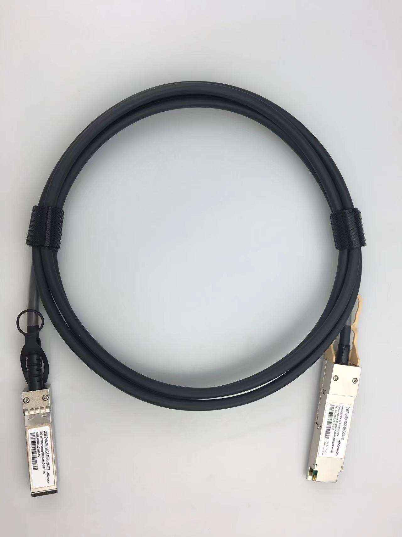
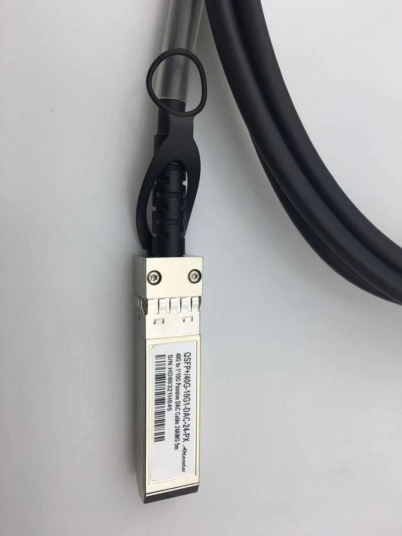
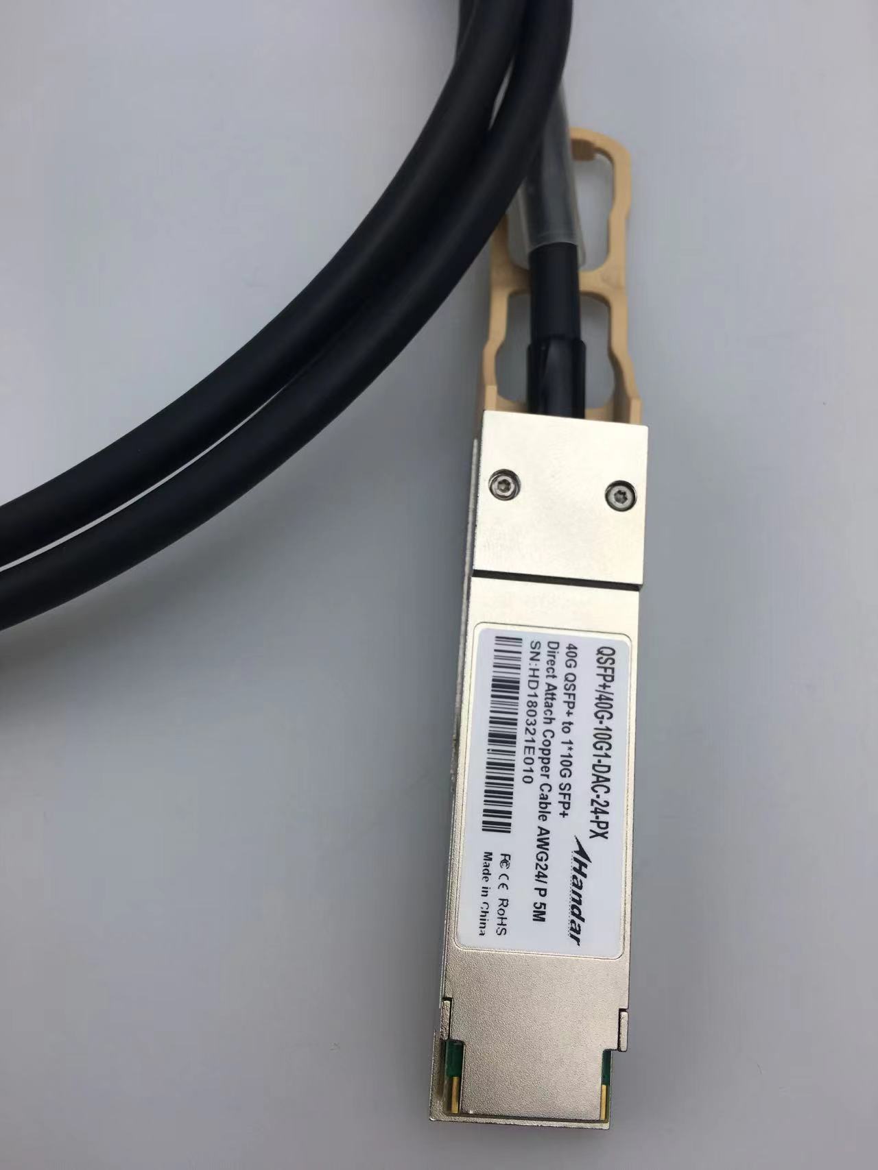
QSFP+/40G-10G1-DAC-24-PX 5m
Support hotline:
0755-86654236 /
Product Details
Product Description
1. Applications
Ø 40G QSFP+ to 10G SFP+
Ø 10G/40Gigabit Ethernet
Ø InfiniBand4x SDR, DDR, QDR
Ø Switches, Routers, and HBAs
Ø Data Centers
2. Features
Ø Hybrid cable conforms to the Small Form Factor SFF-8436 and SFF-8431
Ø Support for multi-gigabit data rates :1 Gb/s - 10 Gb/s (per channel)
Ø Maximum aggregate data rate: 40 Gb/s (4 x 10Gb/s)
Ø Hybrid cable link length up to 5m (passive limiting)
Ø High-Density QSFP 38-PIN and SFP 20-PIN Connector
Ø Power Supply :+3.3V
Ø Low power consumption: 0.02 W (typ.)
Ø Temperature Range: 0~ 70 °C
3. Description
Handar's High Speed 40G QSFP+ to 10G SFP+ Direct Attach Cable copper cable assemblies are a low cost alternative for short reach 4X applications. They are designed to be fully compatible in form factor and optical/electrical connections according to the QSFP Multi-Source Agreement.
QSFP+ connectors provide four channels of data in one pluggable interface. Each channel is capable of transferring data at 10Gbps and supports a total of aggregate 40Gbps as specified for QSFP+. These interconnects have three times the density of SFP+ interconnects(MSA) and have been designed to meet the harshest external operating conditions including temperature, humidity and EMI interference.
QSFP+ cable assemblies are hot swappable and the programmed EEPROM signature enables the host to differentiate between a copper cable assembly and a fiber optic module.
Low power consumption assists in making the passive copper cable assembly an economic solution for withinrack, or rack-to-rack applications.
4. standard
Ø Compliant with electrical standards IEEE 802.3ba
Ø Compliant with mechanical standard SFF-8436 and SFF-8431
Ø Compliant with EEPROM standard SFF-8472
Ø RoHS Compliant
5. Performance Specifications
5.1. Absolute Maximum Ratings
These values represent the damage threshold of the module. Stress in excess of any of the individual Absolute Maximum Ratings can cause immediate catastrophic damage to the module even if all other parameters are within Recommended Operating Conditions.
Table.1 Absolute maximum ratings
Parameter | Symbol | Min | Max | Unit |
Maximum Supply Voltage | Vcc | 0 | 3.6 | V |
Storage Temperature | Ts | -40 | 85 | °C |
Relative Humidity | RH | 5 | 95 | % |
5.2. Recommended Operating Conditions
Table.2 Recommended Operating Conditions
Parameter | Symbol | Min | Typical | Max | Unit |
Operating Case Temperature | Standard Tc | 0 | 25 | 70 | °C |
Storage Temperature | Ts | 0 | 70 | °C | |
Relative Humidity | RH | 5 | 95 | % | |
Data Rate | 10/40 | Gbps |
Table.3Product Characteristics
Test Type | Test Item | Target | Reference | |
Differential Impedence | 100+/ -10ohm (Rise time of 50 ps (20 %- 80 %)) | IEEE Std.802.3ba | ||
Electrical Characteristics | Differential Mode RL | Frequency(GHz) 0.1-1.0 1.0-4.1 | SDD11 & SDD22(max) -10 -(12-2*sqrt(f)) | Per table 10 of 1B Cable MOL.v 0.68 |
Differential IL | Frequency 100MHz 200MHz 625MHz 1250MHz 1875MHz 2500MHz | SDD21(min) -8 -8 -8.5 -12.1 -14.7 -17 | Ref table 43 ofInfinibandArchitecture Spec, V2 | |
NEXT | ≥26dB @ 10MHz to 5.0GHz | / | ||
Intra-Pair Skew | ≤100 ps(TDT Method) Rise time of 35 ps | (20 %- 80 %) | ||
Intra-Pair Skew | ≤400 ps(TDT Method) Rise time of 35 ps | (20%~80 %) | ||
EnvironmentalCharacteristics
| Operating Temperature | -40~85°C | Cable operating temp.range | |
Thermal Shock | No evidence of physical damage | EIA-364-32 Test | ||
Cyclic Temp. & Humidity | No evidence of physical damage | EIA-364-31 Method III,Test Cond A | ||
Salt spray | 48 hours salt spraying after shell corrosive area less than 5% | EIA-364-26 | ||
Temperature Life | Performance meets the specification requirement | EIA-364-17, Method A, Test Cond 3 at 105°±2°C | ||
MechanicalCharacteristics
| MechanicaIVibration | Performance meets the specification requirement | EIA-364-28E.11 TC-VII, Test Cond. D 15minutes in X,Y,Z axis. | |
Cable Flex | Performance meets the specification requirement | EIA-444-1B | ||
Mechanical Shock | Performance meets the specification requirement | EIA-364-27B, TG-G. 3 times in 6 directions, 100g, 6ms | ||
Cable plug Insertion | 40N Max. | Per QSFP MSA Rev 1.0 | ||
Cable plug extraction | 30N Max. | Per QSFP MSA Rev 1.0. | ||
Latch retention force | 50N Min. No evidence of physical damage | EIA-364-13 | ||
Durability | 50 Time. No evidence of physical damage | EIA-364-09; perform plug&unplug cycles | ||
5.4. Pin Definitions


Table.4SFP Pin Definitions
PIN | Symbol | Description | Remarks |
1 | VEET | Transmitter ground (common with receiver ground) | Circuit ground is isolatedfrom chassis ground |
2 | Tx_Fault | Transmitter Fault. Not supported | |
3 | Tx_Disable | Transmitter Disable. Laseroutput disable on high or open | Disabled: TDIS>2V or open Enabled: TDIS<0.8V |
4 | SDA | 2-wire Serial Interface Data Line | Should Be pulled up with4.7k – 10kohm on hostboard to a voltage between2V and 3.6V |
5 | SCL | 2-wire Serial Interface Clock Line | |
6 | MOD_ABS | Module Absent. Grounded within the module. | |
7 | RS0 | No connection required | |
8 | RX_LOS | Loss of Signal indication. Logic 0 indicates normal operation | LOS is open collector output |
9 | RS1 | No connection required | |
10 | VEER | Receiver ground (common with transmitter ground) | Circuit ground is isolatedfrom chassis ground |
11 | VEER | Receiver ground (common with transmitter ground) | |
12 | RD– | Receiver Inverted DATA out. AC coupled | |
13 | RD+ | Receiver Non-inverted DATA out. AC coupled | |
14 | VEER | Receiver ground (common with transmitter ground) | Circuit ground is isolatedfrom chassis ground |
15 | VCCR | Receiver power supply | |
16 | VCCT | Transmitter power supply | |
17 | VEET | Transmitter ground (common with receiver ground) | Circuit ground is isolatedfrom chassis ground |
18 | TD+ | Transmitter Non-Inverted DATA in. AC coupled | |
19 | TD– | Transmitter Inverted DATA in. AC coupled | |
20 | VEET | Transmitter ground (common with receiver ground) | Circuit ground is isolatedfrom chassis ground |

Table.5QSFP Pin Definitions
Pin number | Logic | Symbol | Signal | Description |
1 | GND | Signal Ground | Ground | |
2 | CML-I | Tx2n | Tx2n | Transmitter Inverted Date Input.AC coupled |
3 | CML-I | Tx2p | Tx2p | Transmitter Non_Inverted Date Input.AC coupled |
4 | GND | Signal Ground | Ground | |
5 | CML-I | Tx4n | Tx4n | Transmitter Inverted Date Input.AC coupled |
6 | CML-I | Tx4p | Tx4p | Transmitter Non_Inverted Date Input.AC coupled |
7 | GND | Signal Ground | Ground | |
8 | LVTTL-I | ModSelL | ModSelL | Module Select pin.Selected when held low by the host. |
9 | LVTTL-I | ResetL | LPMode_Reset | Module Reset.A"low" pulse induces a reset on the module. |
10 | Vcc Rx | Vcc Rx | +3.3V Power Supply Receiver | |
11 | LVCMOS-I/O | SCL | SCL | 2-wire serial interface |
12 | LVCMOS-I/O | SDA | SDA | |
13 | GND | Signal Ground | Ground | |
14 | CML-O | Rx3p | Rx3p | Receiver Non_Inverted Date Input.AC coupled |
15 | CML-O | Rx3n | Rx3n | Receiver Inverted Date Input.AC coupled |
16 | GND | Signal Ground | Ground | |
17 | CML-O | Rx1p | Rx1p | Receiver Non_Inverted Date Input.AC coupled |
18 | CML-O | Rx1n | Rx1n | Receiver Inverted Date Input.AC coupled |
19 | GND | Signal Ground | Ground | |
20 | GND | Signal Ground | Ground | |
21 | CML-O | Rx2n | Rx2n | Receiver Inverted Date Input.AC coupled |
22 | CML-O | Rx2p | Rx2p | Receiver Non_Inverted Date Input.AC coupled |
23 | GND | Signal Ground | Ground | |
24 | CML-O | Rx4n | Rx4n | Receiver Inverted Date Input.AC coupled |
25 | CML-O | Rx4p | Rx4p | Receiver Non_Inverted Date Input.AC coupled |
26 | GND | Signal Ground | Ground | |
27 | LVTTL-O | ModPrsL | ModPrsL | Module Present pin.Internally grounded inside the module. |
28 | LVTTL-O | IntL | IntL | Interrupt by the QSFP module."Low"indicates an Alarm/Warning. |
29 | Vcc Tx | Vcc Tx | +3.3V Power Supply Transmitter | |
30 | Vccl | Vccl | +3.3V Power Supply | |
31 | LVTTL-I | LPMode | LPMode | Low Power Mode |
32 | GND | Signal Ground | Ground | |
33 | CML-I | Tx3p | Tx3p | Transmitter Non_Inverted Date Input.AC coupled |
34 | CML-I | Tx3n | Tx3n | Transmitter Inverted Date Input.AC coupled |
35 | GND | Signal Ground | Ground | |
36 | CML-I | Tx1p | Tx1p | Transmitter Non_Inverted Date Input.AC coupled |
37 | CML-I | Tx1n | Tx1n | Transmitter Inverted Date Input.AC coupled |
38 | GND | Signal Ground | Ground | |
Housing | Chassis Ground |
5.6. Mechanical Dimensions

Diagram of Mechanical Dimensions
6. Application Cautions
6.1. ESD
This transceiver is specified as ESD threshold 1kV for high speed pins and 2kV for all other electrical input pins, tested per MIL-STD-883, Method 3015.4 /JESD22-A114-A (HBM). However, normal ESD precautions are still required during the handling of this module. This transceiver is shipped in ESD protective packaging. It should be removed from the packaging and handled only in an ESD protected environment.
6.2. LASER SAFTY
This is a Class 1 Laser Product according to IEC 60825-1:1993:+A1:1997+A2:2001. This product complies with 21 CFR 1040.10 and 1040.11 except for deviations pursuant to Laser Notice No. 50, dated (July 26, 2001)
6.3. Important Notice

Note:
1)Copper type maximum length recommended at 15 meters;
2)Various cable lengths available for all types;
3)Latch/tab available”on top”or”bottom”position.
7. Order Information
Part No. | Description | Rate | Length | Wire Gauge |
HD-QSFP+/40G-10G1-DAC-24-P3 | 40G QSFP+ to 10G SFP+ DAC Passive | 40G/ 1x 10.3G | 3 meter | AWG24 |
HD-QSFP+/40G-10G1-DAC-24-P5 | 40G QSFP+ to 10G SFP+ DAC Passive | 40G/ 1x 10.3G | 5 meter | AWG24 |
MenuProduct center
- 1X9 optical module
- 1.25G 2.5G 3G SFP optical module
- Video SFP High-definition video dedicated SFP optical module
- 10G SFP+ Optical Module
- 25G 40G 100G 400G high speed optical module
- DAC AOC Direct Cable
- Media Converters & Industrial Switches


 sales@huahanda.com
 0755-86654236