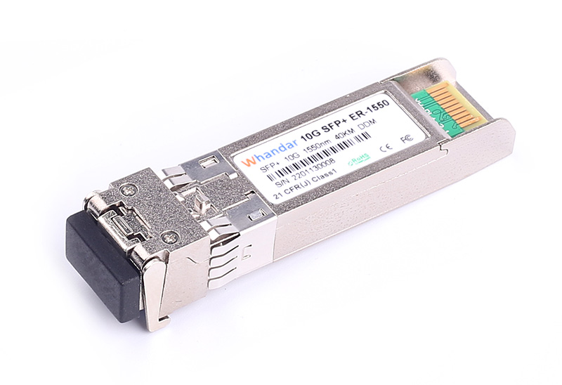
产品介绍
产品特性
1、热插拔SFP封装
2、双纤LC接口
3、采用EML激光器件
4、在单模光纤中传输距离达到40千米
5、内置数字诊断功能
6、符合SFP MSA标准
7、+3.3V单供电电压
8、符合RoHS 6标准
9、工作温度范围:
商业级:0 to +70°C
工业级:-40 to +85°C
兼容性强,适用于国内外各品牌交换机
产品应用
万兆以太网
光纤网络OC-192 同步数字体系STM-64
万兆交换机互联
万兆路由/服务器光链接
其他万兆光传输系统
光学参数
Parameter | Symbol | Min. | Typical | Max. | Unit | Note |
Transmitter Section: |
Center Wavelength | λt | 1530 |
| 1565 | nm |
|
Spectral Width (-20dB) | σ |
|
| 0.3 | nm |
|
Side Mode Suppression Ratio | SMSR | 30 | - | - | dB |
|
Average Optical Power | Pavg | -3 |
| +4.0 | dBm |
|
Optical Power OMA | Poma | -2.1 | - | - | dBm |
|
Laser Off Power | Poff | - | - | -30 | dBm |
|
Extinction Ratio | ER | 6.0 | - | - | dB |
|
Transmitter Dispersion Penalty | TDP | - | - | 3.2 | dB |
|
Relative Intensity Noise | Rin | - | - | -128 | dB/Hz | 12dB reflection |
Optical Return Loss Tolerance |
| - | - | 12 | dB |
|
Receiver Section: |
|
Center Wavelength | λr | 1260 |
| 1620 | nm |
|
Receiver Sensitivity in Average Power | Sen | -15.8 |
| -1.0 | dBm | 1 |
Stressed Sensitivity (OMA) |
| -14.1 | - |
| dBm | 2 |
Stressed Sensitivity (OMA) |
| -11.3 | - |
| dBm | 2 |
Vertical eye closure penalty |
| 2.2 | - | - | dB | 3 |
Los Assert | LosA | -30 | - | - | dBm |
|
Los Dessert | LosD | - | - | -16 | dBm |
|
Los Hysteresis | LosH | 0.5 | - | - | dB |
|
Overload | Pin | - | - | 0.5 | dBm | 1 |
Receiver Reflectance |
| - | - | -12 | dB |
|
Stressed eye jitter |
| 0.3 | - | - | UIp-p | 2 |
Receive electrical 3dB upper cutoff frequency |
| - | - | 12.3 | GHz |
|
Receiver power (damage) |
| - | - | 1.5 | dBm |
|
Notes:
1. Average optical power shall be measured using the methods specified in TIA/EIA-455-95.
2. Receiver sensitivity is informative. Stressed receiver sensitivity shall be measured with conformance test signal for BER =1x 10-12 .
3. Vertical eye closure penalty and stressed eye jitter are the test conditions for measuring stressed receiver sensitivity. They are not the required characteristic of the receiver.
4. Power budget is defined as the different between the Rx sensitivity and the Tx output power of the interface.
5. Path penalty is intended as the power penalty of the interface between back-to-back and the maximum applied dispersion.
引脚定义


PIN | Logic | Symbol | Name / Description | Note |
1 |
| VeeT | Module Transmitter Ground | 1 |
2 | LVTTL-O | TX_Fault | Module Transmitter Fault |
|
3 | LVTTL-I | TX_Dis | Transmitter Disable; Turns off transmitter laser output |
|
4 | LVTTL-I/O | SDA | 2-Wire Serial Interface Data Line | 2 |
5 | LVTTL-I | SCL | 2-Wire Serial Interface Clock | 2 |
6 |
| MOD_DEF0 | Module Definition, Grounded in the module |
|
7 | LVTTL-I | RS0 | Receiver Rate Select |
|
8 | LVTTL-O | RX_LOS | Receiver Loss of Signal Indication Active LOW |
|
9 | LVTTL-I | RS1 | Transmitter Rate Select (not used) |
|
10 |
| VeeR | Module Receiver Ground | 1 |
11 |
| VeeR | Module Receiver Ground | 1 |
12 | CML-O | RD- | Receiver Inverted Data Output |
|
13 | CML-O | RD+ | Receiver Data Output (not used) |
|
14 |
| VeeR | Module Receiver Ground | 1 |
15 |
| VccR | Module Receiver 3.3 V Supply |
|
16 |
| VccT | Module Receiver 3.3 V Supply |
|
17 |
| VeeT | Module Transmitter Ground | 1 |
18 | CML-I | TD+ | Transmitter Non-Inverted Data Input |
|
19 | CML-I | TD- | Transmitter Inverted Data Input |
|
20 |
| VeeT | Module Transmitter Ground | 1 |
Notes:
1. Module ground pins GND are isolated from the module case.
2. Shall be pulled up with 4.7K-10Kohms to a voltage between 3.15V and 3.45V on the host board.
订购信息
Part Number | Product Description |
HD-SFP+/10G-ER-1550 | 1550nm, 10Gbps, 40Km, SFP+ Transceiver 0ºC ~ +70ºC . |
HD-SFP+/10G-ER-1550I | 1550nm, 10Gbps, 40Km, SFP+ Transceiver -40ºC ~ +85ºC . |


 0755-86654236