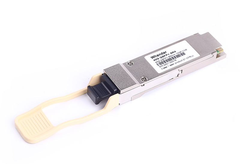
产品介绍
产品特性
◆ 热插拔QSFP封装
◆ 最高支持41.25Gbps传输速率
◆ 独立4通道,单通道支持1.06Gb/s 至10.5Gb/s多种速率
◆ 在OM3多模光纤中传输距离达到100米, 在OM4多模光纤中传输距离达到150米
◆ MPO-12接口
◆ 低功耗<1.5 W
◆ +3.3V单电源供电
◆ 内置数字诊断功能
◆ 工作温度范围:0°C 至 70°C
◆ 符合 RoHS 6 标准
产品应用
◆ 40GBASE-SR4 40G Ethernet
◆ 40G-IB-QDR /20G-IB-DDR / 10G-IB-SDR InfniBand
◆ Breakout to 4 x 10GBASE-SR
◆ Proprietary interconnections
光学参数/Optical Transmitter Characteristics |
Parameter | Symbol | Min | Typical | Max | Unit | Notes |
Center Wavelength | λout | 840 | 850 | 860 | nm |
|
Average Launch Power each lane | Pout | -7.6 |
| 2.4 | dBm |
|
Difference in Power between any two lanes [OMA] | DPX |
|
| 4.0 | dB |
|
Peak Power per Lane | PPX |
|
| 4.0 | dBm |
|
Spectral Width (RMS) | σ |
|
| 0.65 | nm |
|
Optical Extinction Ratio | ER | 3.0 |
|
| dB |
|
Transmitter and Dispersion Penalty each lane | TDP |
|
| 3.5 | dB |
|
Optical Return Loss Tolerance | ORL |
|
| 12 | dB |
|
Average launch power of OFF transmitter, per lane |
|
|
| -30 | dBm |
|
Transmitter eye mask definition{X1,X2,X3,Y1,Y2,Y3} | {0.23,0.34,0.43,0.27,0.35,0.4} |
|
Optical Receiver Characteristics |
Parameter | Symbol | Min | Typical | Max | Unit | Notes |
Receiver Wavelength | λin | 840 |
| 860 | nm |
|
Average Receive Power per Lane | RXPx | -9.5 |
| 2.4 | dBm |
|
Stressed Receiver Sensitivity in OMA | SRS |
|
| -5.4 | dBm | 1 |
LOS Assert | LOSA | -30 |
|
| dBm |
|
LOS De-Assert | LOSD |
|
| -12 | dBm |
|
LOS Hysteresis |
| 0.5 |
|
| dB |
|
Receiver Reflectance | Rfl |
|
| -12 | dB |
|
Notes:
1.Measured with a PRBS 231-1 test pattern, @10.3125Gb/s, BER<1E-12.
引脚定义
Pin | Symbol | Name/Description | Notes |
1 | GND | Transmitter Ground | 1 |
2 | Tx2n | Transmitter Inverted Data Input |
|
3 | Tx2p | Transmitter Non-Inverted Data output |
|
4 | GND | Transmitter Ground | 1 |
5 | Tx4n | Transmitter Inverted Data Input |
|
6 | Tx4p | Transmitter Non-Inverted Data output |
|
7 | GND | Transmitter Ground | 1 |
8 | ModSelL | Module Select |
|
9 | ResetL | Module Reset |
|
10 | VccRx | 3.3V Power Supply Receiver | 2 |
11 | SCL | 2-Wire serial Interface Clock |
|
12 | SDA | 2-Wire serial Interface Data |
|
13 | GND | Receiver Ground | 1 |
14 | Rx3p | Receiver Non-Inverted Data Output |
|
15 | Rx3n | Receiver Inverted Data Output |
|
16 | GND | Receiver Ground | 1 |
17 | Rx1p | Receiver Non-Inverted Data Output |
|
18 | Rx1n | Receiver Inverted Data Output |
|
19 | GND | Receiver Ground | 1 |
20 | GND | Receiver Ground | 1 |
21 | Rx2n | Receiver Inverted Data Output |
|
22 | Rx2p | Receiver Non-Inverted Data Output |
|
23 | GND | Receiver Ground | 1 |
24 | Rx4n | Receiver Inverted Data Output |
|
25 | Rx4p | Receiver Non-Inverted Data Output |
|
26 | GND | Receiver Ground | 1 |
27 | ModPrsl | Module Present |
|
28 | IntL | Interrupt |
|
29 | VccTx | 3.3V power supply transmitter | 2 |
30 | Vcc1 | 3.3V power supply | 2 |
31 | LPMode | Low Power Mode,not connect |
|
32 | GND | Transmitter Ground | 1 |
33 | Tx3p | Transmitter Non-Inverted Data Input |
|
34 | Tx3n | Transmitter Inverted Data Output |
|
35 | GND | Transmitter Ground | 1 |
36 | Tx1p | Transmitter Non-Inverted Data Input |
|
Notes:
1.GND is the symbol for signal and supply (power) common for the QSFP+ module. All are common within the QSFP+ module and all module voltages are referenced to this potential unless otherwise noted. Connect these directly to the host board signal-common ground plane.
2.Vcc Rx, Vcc1 and Vcc Tx are the receiver and transmitter power supplies and shall be applied concurrently. Requirements defined for the host side of the Host Edge Card Connector are listed in Table 6. Recommended host board power supply filtering is shown in Figures 3 and 4. Vcc Rx Vcc1 and Vcc Tx may be internally connected within the QSFP+ Module in any combination. The connector pins are each rated for a maximum current of 500 mA.

Figure 1.Electrical Pin-out Details
订购信息
Part. No |
| Specifications |
Pack | Rate* (Gbps) | Po (dBm) | RX | Sen* (dBm) | Temp (℃) | Reach (m) | Pull tap Color | DDM |
HD-QSFP+/40G-SR4 | QSFP+ | 4*10.3125 | -7.6~2.4 | PIN | <-9.5 | 0~+70 | 150 | Beige | Y |
*Note:
Measured with a PRBS 231-1 test pattern, @10.3125Gb/s, BER<1E-12. 2.Receiver sensitivity in OMA


 0755-86654236