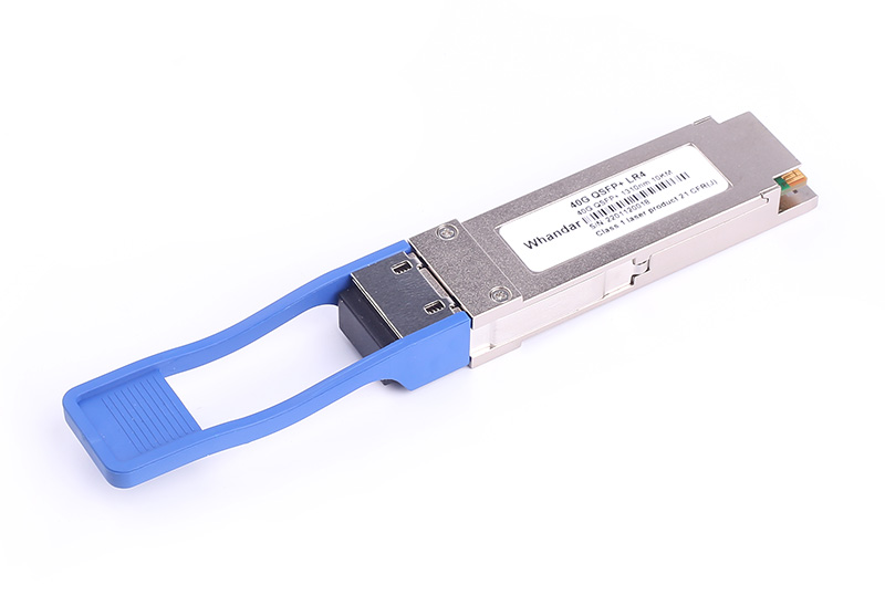
Product Description
1 Features
Duplex LC connector
Hot-pluggable QSFP+ form factor
Operating data rate up to11.3Gbps per Lane
Up to 10km transmission
Maximum 3.5W operation power
Compliant with IEEE 802.3ba Compliant with SFF 8436
Built-in Digital Diagnostic Monitoring (DDM) functions
Complies with RoHS directive (2002/95/EC)
Single +3.3V power supply operating
2 Applications
40GBASE-LR4 40G Ethernet
3 Optical Characteristics
Transmitter Characteristics
Parameter | Symbol | Min. | Typ. | Max. | Unit | Note |
Signal Speed per lane | Sp |
| 10.3125 |
| Gbps |
|
Center Wavelength | l | 1264.5 | 1271 | 1277.5 | nm | Lane0 |
1284.5 | 1291 | 1297.5 | nm | Lane1 |
1304.5 | 1311 | 1317.5 | nm | Lane2 |
1324.5 | 1331 | 1337.5 | nm | Lane3 |
Spectral Width (-20dB) | Dl | - | - | 1 | nm |
|
Side Mode Suppression Ratio | SMSR | 30 | - | - | dB |
|
Total Output Optical Power | Pot |
|
| 8.3 | dBm |
|
Average Optical Output Power | Po | -7 | - | 2.3 | dBm |
|
Optical Modulation Amplitude, Each Lane | OMA | -4 |
| 3.5 | dBm |
|
Extinction Ratio | Er | 3.5 | - | - | dB |
|
Differential Input Impedance | - | 80 | 100 | 120 | Ω |
|
Differential Data Input Swing | VINPP | 120 |
| 1000 | mV |
|
Receiver Characteristics
Parameter | Symbol | Min. | Typ. | Max. | Units | Notes |
Wavelength of Operation | l | 1264.5 | 1271 | 1277.5 | nm | Lane0 |
1284.5 | 1291 | 1297.5 | nm | Lane1 |
1304.5 | 1311 | 1317.5 | nm | Lane2 |
1324.5 | 1331 | 1337.5 | nm | Lane3 |
Optical Input Power, each lane | Pin | -13.7 | - | 2.3 | dBm | 4.4.1 |
Damage Threshold | Pmax | - | - | 3.3 | dBm |
Receiver Sensitivity (OMA), each Lane | Rxsen |
|
| -11.5 | dBm |
Differential Data Output Swing | VOUTPP | 350 |
| 800 | mV |
|
Note4.4.1: Measured with 10.3125Gbps, BER=1x10-12
Digital Diagnostic Monitoring Characteristics
Parameter | Symbol | Range | Accuracy |
Transceiver Case Temperature | T | Measured transceiver case temperature over specified operating range | ±3°C |
Supply Voltage | Vcc | Internally measured transceiver supply voltage ,3.0~3.6V | ±3% |
TX Bias Current | Id | Measured TX Bias current in uA | ±10% |
TX Output Power | Po | Measured TX Output Power in dBm Over the specified output power range | ±3dB |
Received Optical Power | Pi | Measured RX Received Power in dBm Over the specified input power range | ±3dB |
4 Pin Definitions
Pin Diagram

Pin Descriptions
Pin# | Logic | Name | Function | Notes |
1 |
| GND | Ground |
|
2 | CML-I | Tx2n | Transmitter Inverted Data Input |
|
3 | CML-I | Tx2p | Transmitter Non-Inverted Data output |
|
4 |
| GND | Ground |
|
5 | CML-I | Tx4n | Transmitter Inverted Data Input |
|
6 | CML-I | Tx4p | Transmitter Non-Inverted Data output |
|
7 |
| GND | Ground |
|
8 | LVTLL-I | ModSelL | Module Select |
|
9 | LVTLL-I | ResetL | Module Reset |
|
10 |
| VccRx | +3.3V Power Supply Receiver |
|
| Pin# | Logic | Name | Function |
31 | LVTTL-I | LPMode | Low Power Mode |
32 |
| GND | Ground |
33 | CML-I | Tx3p | Transmitter Non-Inverted Data Input |
34 | CML-I | Tx3n | Transmitter Inverted Data Output |
35 |
| GND | Ground |
36 | CML-I | Tx1p | Transmitter Non-Inverted Data Input |
37 | CML-I | Tx1n | Transmitter Inverted Data Output |
38 |
| GND | Ground |
5 Ordering Information
Part Number | Operating Case Temperature | RoHS Compliant |
HD-QSFP+/40G-LR4 | 0 ~ 70 °C | RoHS-6 |
HD-QSFP+/40G-LR4-I | -40 ~ 85 °C | RoHS-6 |

6 Document History
Version | Change Description | Changed by | Date |
VER A | Initial Release | Wang Xin | 01/15/2021 |


 sales@huahanda.com
 0755-86654236